Electron microscopy has been of a multi-facet use in this technologically driven era. They have made the process of image processing far easier. Tem and Sem are two different types of electron microscopy techniques in use today. It may be difficult to find out the differences between the two. However, the two are considerably different.
Key Takeaways
- TEM (Transmission Electron Microscopy) offers better resolution than SEM (Scanning Electron Microscopy).
- SEM generates surface images, while TEM produces images of the internal structure of a sample.
- SEM is easier to use and requires less sample preparation compared to TEM.
Tem vs Sem
TEM is a type of electron microscopy where the electrons pass through the sample and form an image on a fluorescent screen or detector. SEM, is a type of electron microscopy where the electrons scan across the surface of the sample and create an image by detecting the emitted secondary electrons.

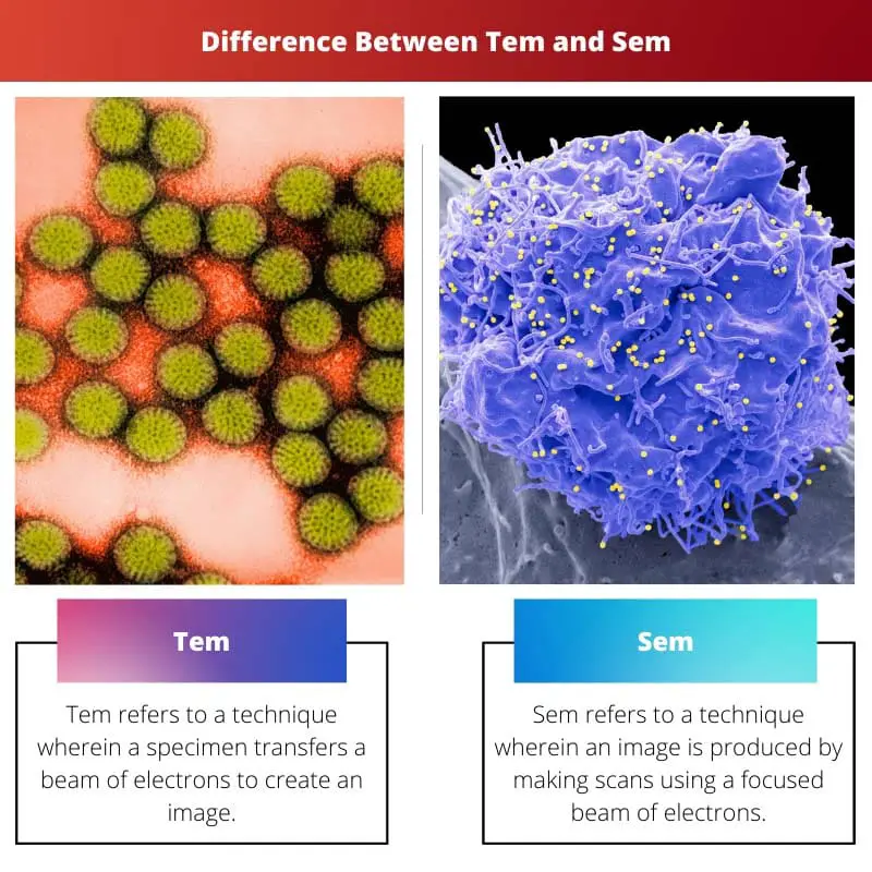
Tem refers to a technique wherein a specimen transfers a beam of electrons to create an image. There are several modes of operation in Tem. Some of these are scanning TEM images, conventional imaging, spectroscopy, diffraction, and a combination of those. In addition, it is possible to further enhance the potential of tem by a series of stages and detectors.
Sem refers to a technique wherein an image is produced by making scans using a focused beam of electrons. The pattern to scan the electron beam is a raster scan. Sem allows an individual to see the surface of any material ranging from biological samples to geological specimens. Moreover, sem may have artificial colouration to give off an aesthetic effect.
Comparison Table
| Parameters of Comparison | Tem | Sem |
|---|---|---|
| Full Form | Tem stands for Transmission Electron Microscopy. | Sem stands for Scanning Electron Microscope. |
| Founder | The credits of the first TEM go to Max Knoll and Ernst Ruska in 1931. | The credits of early scanning microscopy goes to McMullan. |
| Applications | TEM has a practical approach in the field of chemical, physical, and biological sciences. | Sem allows an individual to see the surface of any material ranging from biological samples to geological specimens. |
| Specifications | Tem enables users to observe internal details of a sample. | Sem is a convenient option to scan the surface details of a specimen. |
| Sample Range | Tem can scan only a limited range of specimens. | Sem can scan a wide range of samples. |
What is Tem?
Tem stands for Transmission Electron Microscopy. In this microscopy technique, a specimen transfers a beam of electrons to create an image. Transmission Electron Microscopes are significantly superior to light microscopes as they can image at a comparatively higher resolution. As a result, the device can take into account every minute detail of an item.
TEM has a practical approach in the field of chemical, physical, and biological sciences. It is a technique of extensive use in the fields of virology, material sciences, cancer research, nanotechnology, pollution, palynology, palaeontology, and semiconductor research. Thus, TEM has multiple uses in the modern world.
There are several modes of operation in Tem. Some of these are scanning TEM images, conventional imaging, spectroscopy, diffraction, and a combination of those. Observed closely, any TEM image is a collection of poliovirus. The credits for the first TEM go to Max Knoll and Ernst Ruska in 1931. TEM is also regarded as an essential item in the field of nanoscience.
A tem consists of a vacuum system, specimen stage, electron gun, electron gun, and apertures. Moreover, there are several imaging methods in tem. It is possible to further enhance the potential of tem by a series of stages and detectors. To conclude, tem has become a technique of common use in the present.

What is Sem?
Sem stands for Scanning Electron Microscope. This technique produces an image by making scans using a focused beam of electrons. The pattern to scan the electron beam is a raster scan. There are a few sems that have the potential to achieve a resolution that is way better than 1 nanometer.
In a Sem, the sample observation occurs in a high vacuum, a low vacuum, or wet conditions. The credits of early scanning microscopy go to McMullan. The image production in a sem is an outcome of the interaction of the electron beam with atoms. Various types of signals come into being in the sem.
Sem allows an individual to see the surface of any material ranging from biological samples to geological specimens. Sem is a fast scanner that provides accurate details. It also enables an individual to make observations with little or no sample preparation. Although sem doesn’t provide 3D images, it allows a user to obtain 3D data using several methods.
Sem has been used to measure the roughness of ice crystals. Some other practical applications of sem are in examining the fracture surface of metals, corrosion measurement, fractal dimension, and dimensional measurements. Sem may have artificial colouration to give off an aesthetic effect. To conclude, Sem has a wide variety of uses in the practical arena.

Main Differences Between Tem and Sem
- Tem stands for Transmission Electron Microscopy. In contrast, Sem stands for Scanning Electron Microscope.
- Tem can scan only a limited range of specimens. On the other hand, sem can scan a wide range of samples.
- The credits for the first TEM go to Max Knoll and Ernst Ruska in 1931. In contrast, the credits of early scanning microscopy go to McMullan.
- Tem enables users to observe the internal details of a sample. On the other hand, sem is a convenient option to scan the surface details of a specimen.
- TEM has a practical approach in the field of chemical, physical, and biological sciences. In contrast, Sem allows an individual to see the surface of any material ranging from biological samples to geological specimens.

- https://www.sciencedirect.com/science/article/pii/S0091679X04740170
- https://www.sciencedirect.com/science/article/pii/S0166516218311571

TEM and SEM are valuable tools for scientists and researchers, enabling them to explore the intricate details of various specimens and materials, leading to new discoveries and advancements.
The extensive use of TEM and SEM in various scientific fields underscores the importance of electron microscopy in enabling detailed examination and understanding of a wide range of natural and synthetic materials.
The development of SEM and TEM has significantly contributed to the advancement of scientific research, allowing for in-depth analysis and visualization of the micro- and nano-world.
I appreciate the comparison table provided, which clearly outlines the differences between TEM and SEM, making it easier to understand the unique capabilities of each technique.
TEM and SEM are two important types of electron microscopy that play a significant role in various scientific fields, especially in nanotechnology and virology.
Scanning Electron Microscopy (SEM) is essential for examining surface structures and obtaining detailed information about the topography and composition of a wide range of materials.
The practical applications of TEM and SEM in fields such as virology, nanotechnology, and materials sciences highlight the versatility and significance of electron microscopy technologies.
It’s fascinating to see how electron microscopy techniques have advanced and are now being used across multiple scientific disciplines, from nanotechnology to biology and materials science.
The ability of SEM to provide high-resolution surface images and the detailed internal structure revealed by TEM demonstrate the complementary nature of these two electron microscopy techniques.
Transmission Electron Microscopy (TEM) has revolutionized our ability to observe even the most minute details of a sample, making it a valuable tool in research and scientific analysis.